North America

Research & In-house PCB Prototyping

Shaping the future of technology

In the development of new products, fast iterations are required. The machines and equipment from LPKF Laser & Electronics give you all the possible options for PCB prototyping and micro material processing. Find out all about the systems and processes with which LPKF helps its customers succeed.

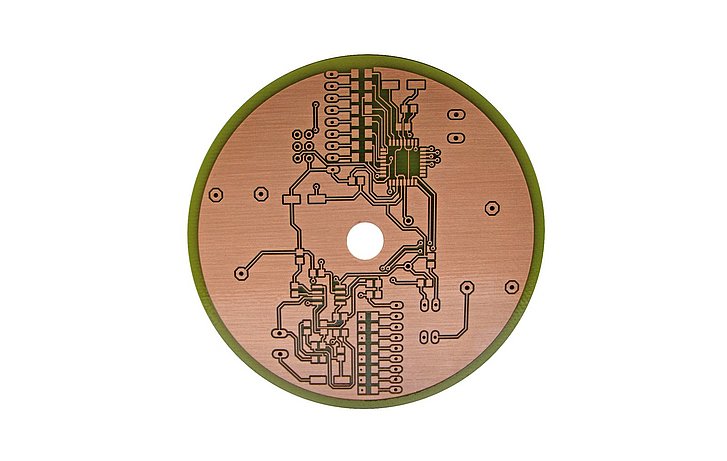
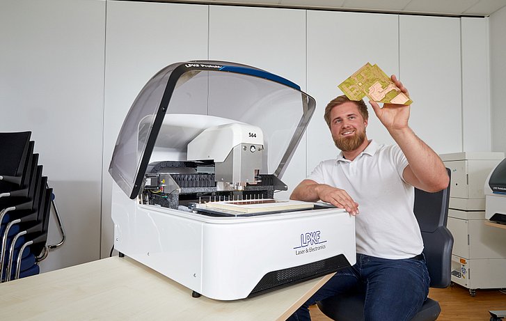
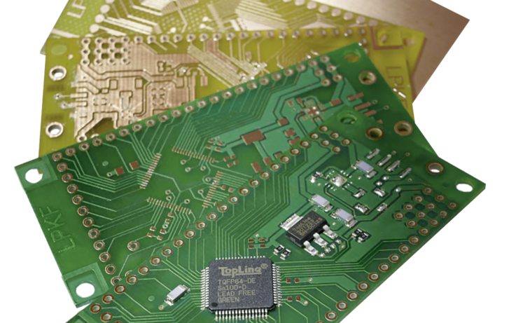
In-house production of printed circuit board prototypes

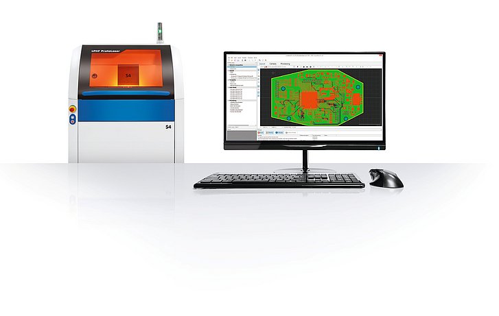
In the development of new products, the time factor is critical. Security of in-house data also plays a major role. From idea to mass-produced goods in minimal time with in-house rapid PCB prototyping. Develop a printed circuit board, manufacture it in just one day, and keep all data in-house: can this be done even faster and more securely?

Micro material processing

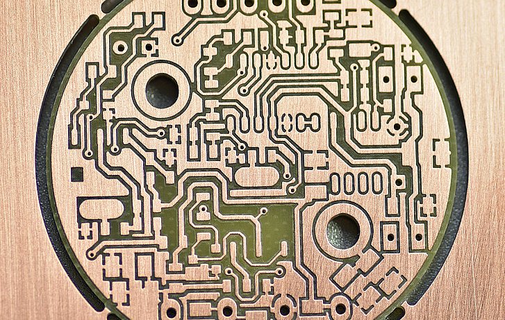
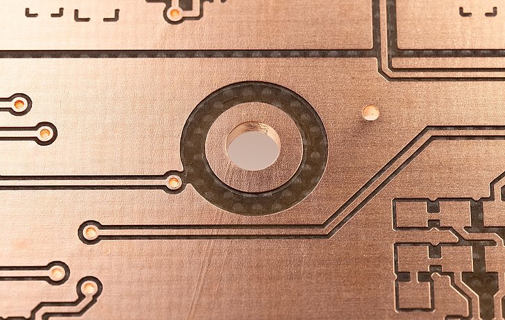
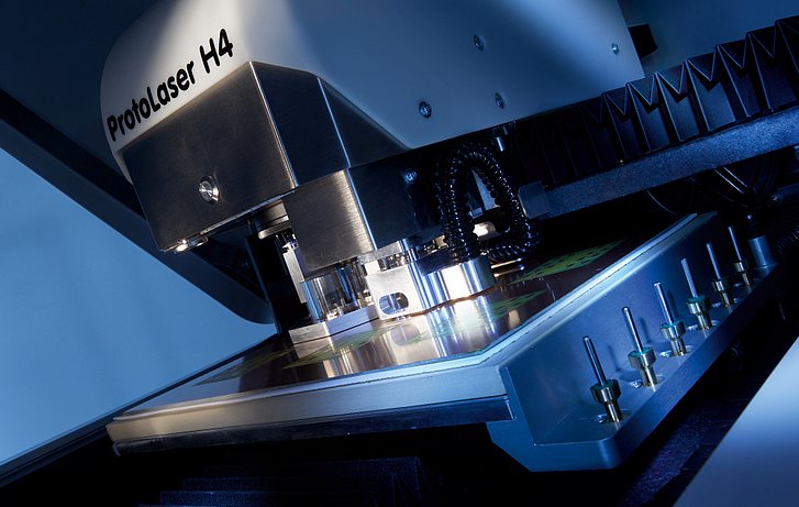
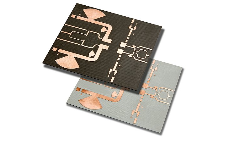
Development of electronic components has been progressing at an astounding pace for years. Integrated circuits are becoming more compact, and at the same time clock speeds are increasing. High frequencies, steep rising edges, and minimal space place huge demands on the printed circuit board. The response has been to use new substrate materials, which are much more difficult to process than the standard FR4 material is. Laser systems from LPKF Laser & Electronics are universal tools for micro material processing, but they can do much more than just machine substrates for printed circuit boards!

ProtoLaser Direct Laser Structuring Systems

Learn more about the structuring of finest conductive path patterns.

High Precision PCB Milling Systems

From design to finished circuit board in just a few hours.

Virtual 3D Product Showroom

Get an overview of the product portfolio and visit special focus rooms.

Micro Material Processing in the Lab

On the right track to innovation.

Process Steps for PCB Prototyping

Coordinated processes from a single source.

Multilayers

Produce up to eight layers in-house.

[Translate to USA:] In-house research for medical components using direct laser processing.
Medical Research

In-house research for medical components using direct laser processing.

LPKF Webinars at a Glance

Learn about upcoming events and webinar recordings on the LPKF webinar channel.

Why In-house PCB Prototyping?

Advantages and application areas for PCB prototyping.

Process Steps for PCB Prototyping

Software with Intuitive Operation

Simple thanks to data preparation and manufacturing process.

PCB Structuring

Generate conductive traces within minutes using mechanical systems and laser processes.

PCB Drilling

Produce through-holes and blind vias.

Through-hole Plating Processes

Work with no chemicals and by electroplating.

PCB Depaneling

Depanel PCBs made from a variety of materials.

SMT / Finishing

Populate PCB prototypes and low volumes.

Logo: LPKF Laser & Elektronics