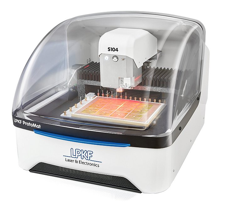
Prototyping with LPKF ProtoMat systems
LPKF Laser & Electronics' benchtop prototyping systems produce high-performance boards that match or exceed the quality of outsourced PCB prototypes. With an LPKF ProtoMat® PCB milling machine, prototype PCBs can be made and tested within a single day - without the use of hazardous and messy chemical etching tanks. Any problems with the initial design can be identified early, allowing for revisions 2 & 3 to be completed in the same day!
"Thanks to our LPKF ProtoMat we took a project that should have taken 10 weeks and did it in only one week."
— Paul Clark from Honeywell C&K Systems
LPKF PCB prototyping systems work directly from CAD data which provides the necessary versatility needed for working on a multitude of various projects, from PCBs to RF enclosures, contour routing, controller housings, faceplates, signs, inspection templates, test fixtures, and even solder paste stencils.
Benefits
- Reduce R&D time, and thus overall time-to-market
- Keep designs confidential and in-house
- Freedom to create and experiment quickly and inexpensively
- Rework, adjust, trim and tune existing PCB's
- Compatibility to any CAD program using standardized file formats
- Mill, drill, and route - the ProtoMat® functions as a PCB router and circuit tracer
- Convenience right in your own lab
Features and options
- Automatic tool change - start your project and come back to a finished board
- Fiducial positioning camera - automatic alignment and reload
- Vacuum table - secures thin or wavy materials
- Through-hole plating
- Multilayer lamination
- Auxiliary SMT assembly equipment (pick & place, stencil printer, and reflow oven)
What does it mean for me?
- Students learn all steps from design to production
- &Faculty research projects
- Expose students to tools used in the commercial industry
- Save $$$
- Numerous design revisions in just one day.
- Trim and tune filters and antennas.
- Create 2.5D aluminum RF housings.
- Create custom shielding, or 3D scribe-and-fold structures.
- Works on a variety of materials from FR4 to Teflon and unfired ceramics.
- Use simulation software more effectively.
- Keep sensitive design data safely in-house
- Avoid the outsource procurement process
- Works with analog, digital, RF and MW designs and substrates for sharring between various groups or departments
- LPKF is a GSA Contractor in the USA
- Not just PCBs: create stencils, housings, faceplates and mechanical parts too.
- Use for production of low-volume quantities.
- Speed is your advantage when competing with the big-boys.
- No more waiting for a prototype to be delivered - fabricate and test in your lab today.
- Multiple applications allow for uses across multiple departments.
- High-mix versatility whether you make one product or hundreds.
- Easily scalable redundancy: multiple machines at various locations, all speaking the same language.
- Quicker prototyping cycles means getting to market before the competition.
- Have a completed prototype in the same time it takes to complete requisition paperwork for outsourcing.


